Mandrel/spacer engineering-based patterning and metallization incorporating metal layer division and rigorously self-aligned vias and cuts (SAVC)
Presented live 27 February 2024
Presentation and Abstract
Authors
Abstract
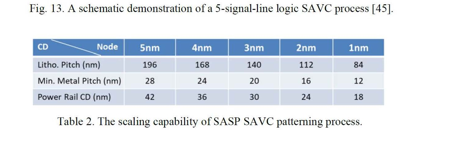
In this paper, we first present a brief review of the advanced-node logic device technology development and its key bottleneck/component processes using the existing lithographic capabilities. It is shown to be feasible to evolve into the GAA era with the minimum change of current FinFET process and a minor refining of previously reported Forksheet structure. The concept of hybrid-channel devices is raised which is not only promising for 3D vertical integration, but also offers an optimal tradeoff between device performance and power/leakage. To address the fabrication challenges, a mandrel/spacer engineering based patterning and metallization technology is proposed and its process development results are reported. This patterning & metallization technique can be applied to fabricate advanced logic and SRAM circuits with significantly enhanced pattern density. It is based on the self-aligned multiple patterning (SAMP) wherein either an alternating arrangement of different materials (with high etching selectivity) or multi-color layer decomposition (i.e., splitting of metallization process) is utilized to solve the edge-placement-error (EPE) issue. In particular, we explore various schemes of self-aligned triple patterning (SATP) to identify the potential solution to ensure a satisfactory profile control of the consecutively formed spacers. Moreover, this technique can incorporate rigorously self-aligned vias & cuts (SAVC), and accommodate a metal-layer division (MLD) to split the neighboring metal lines into two vertically staggered layers with their coupling capacitance significantly reduced. The tested metal Ru allows a direct dry etching, which offers a metal recess capability to enable an alternating-material coverage of neighboring metal wires by two different hard masks such that a selective etching can be applied to form rigorously self-aligned vias. Our early-stage process development is focused on SATP process optimization, fabrication of two simplified grating structures, material screening for appropriate etching selectivity, and metal-layer-division realization. Potential processing challenges such as Ru trench-filling quality and scaling issues of SAVC technology for advanced IC manufacturing will also be discussed.
Presenter
Yijian Chen
Westlake Univ. (China)